4m 100W PA design using a Gemini type dual MOSFET
Although I no longer use this PA, and would recommend instead the SD2931-10 design on the equipment page, the approach here may still be of interest for the free tools and software identified and available on the web, and for the techniques used.Introduction
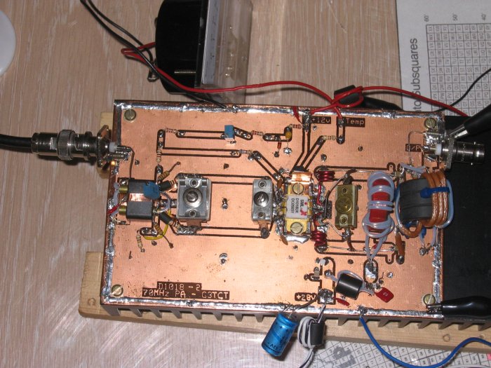
I started this project with the idea of designing a 200W linear for 70MHz based on published designs by Frey . His 50MHz design uses a push pull pair of ARF448A/B high voltage MOSFET devices. These devices are produced in the inexpensive TO247 plastic package and can be purchased at reasonable prices. I redesigned the input and output matching for 70MHz, designed a corresponding PCB, and built and tested a prototype.Before launching into this however I first tried out the design on a lower power device, a dual MOSFET type D1018UK which I had obtained cheaply at a rally. The D1018UK design also uses many of the ideas and components of the Frey design. It shows a gain of almost 20dB, produces 100W output at 70MHz, and runs from a 28v rail. From the datasheet, the D1018 power out is 100W for 5W in with a 28v supply, 13dB gain, ~50% efficiency, Idq=1.2A.
I then produced a design for the pair of ARF448, redesigned the pcb and built the amplifier. I tested it carefully using a 28v rail, but sadly it did not perform – it consumed plenty of dc power, but produced little RF. Then when I tried increasing the rail to 50v, one of the ARF448 went short circuit. Meanwhile the supplier of ARF448s had run out of stock. In my view, the problem with the ARF448 type device is the package. It is not really suitable for a VHF power application where high currents and good balance between the pair is essential, so I would not recommend them for a VHF PA.
This article describes the D1018UK linear, the issues addressed and methods of design and construction. The linear has been in use on 4m, and has been used in several contests.
Circuit description
The circuit is shown here. Q1 is the two halves of the D1018. The bias circuit is from Frey, with the addition of the network R11-R15 to achieve DC balance between the two halves of the device. I found this to be essential – for my device there was ~0.5V difference between the threshold voltages for each gate, and this would result in a significant imbalance in quiescent current.The LM35 is a temperature measurement IC so that the thermal behaviour may be monitored. A 100µA meter is attached between “Temp” and ground. Once behaviour in this respect is satisfactory, it may be omitted.
Thermal design issues
The Frey paper points out that because MOSFETs have a negative temperature coefficient there is a risk of thermal runaway, and linear operation is only possible if a reduced supply voltage is used. Whilst this may apply to the ARF448 devices, the D1018 device with a 28V supply shows no tendency for thermal runaway A substantial heatsink should be used to keep case temperature down and for good reliability. The prototype uses a heatsink measuring 300x100x40mm. This has proved adequate without the use of a fan.Temperature compensation of the bias supply is achieved as in Frey's design by the use of a thermistor T. This is glued to a small piece of copper which is then kept in contact with the D1018 with the retaining screw. This eases maintenance if the MOSFET needs to be removed from the PCB. A smaller value of R2 or a larger value of R4 will increase the thermal sensitivity. Proper operation is indicated when the set value of quiescent current does not change after the heatsink is hot from prolonged operation.
Input Matching
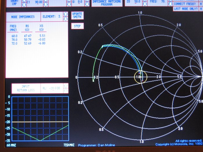
From the datasheet the D1018 has an input impedance of Zin =2.0-j2.2 at 500MHz, representing an input capacitance of 144pF. I have translated this into an impedance of 2.0-j15.7 at 70MHz. The input matching starts with transformer T1 which transforms 50Ω down to 12.5Ω. This is then further reduced via the pi network C1, TL1 and C2 to match the device Zin. Using the Motorola impedance matching program “MIMP” from Circuit Sage (and remembering to include the leakage reactance of T1 of 18nH), the values obtained are:-C1=449pF, transmission line TL with W=100mil, H=59mil, T=1.4mil, Er=5, L=1.616” (41.05mm), and C2=71pF.
I found the gate input circuit had too high a Q and caused the amplifier to oscillate. This is cured by the addition of the components C10/R9 and C11/R10. R9 is formed from three 15ohm 0.5W resistors in parallel, and the same for R10.
It is also most important for amplifier stability to tune the input circuit to match 50ohm input before applying power. I did this by making an impedance bridge. I built the bridge described in the VHF handbook p11.13. I used a 5961 toroid with 6 turns, 350pF variable, 150pF fixed and 100ohm pot. I first tested the bridge by finding the null with a 50ohm dummy load, and then tuned the PA input circuit for the same null. This was quite critical and very difficult to find by any other method. Once I'd done this the PA was stable and I could sort out the output matching.
Circuit Sage has a useful set of resources – in particular the Motorola impedance matching program with in-built Smith chart which seems to have disappeared from Circuit Sage now. It's a rather old program but useful so here is mimp.zip
| NEW! Additional comments added 22 Apr 2014 Mimp is not supported in Windows 7 and 8. To run Mimp, you will need to download and use Dosbox Start Dosbox. At the z: prompt, you will need to mount a drive for your copy of Mimp, eg mount e “c:\my file location\mimp\” [noting that “ is found as keyboard char @] then type e: and mimp To avoid having to type this each time, save the following 2 lines to the config file:- mount e c:\my file location\mimp\ e: Now start by typing mimp. You can make it full screen by typing alt/enter Calculate the series equivalents and enter load values as Rs, Xs which get translated to the parallel values Rp, -Xp [Mimp changes the sign to achieve a conjugate match! Enter Xs as +ve to get Xp -ve] Enter source 50ohm
|
The Smith chart produced by MIMP for the input matching is shown below.
PCB Design and Construction
Caution – MOSFETs are static-sensitive and can be easily destroyed. Always keep them in conductive wrap until ready to solder into circuit. Earth the soldering iron to the board. Wear a wrist strap and earth it to the board. Yes, I found out the hard way too.For schematic design and PCB layout I investigated a number of programs. I found some that were very capable but far too expensive for one-off developments. I also found some that required other operating systems such as Unix, or imposed unacceptable limits on board size. One program that did meet my requirements was the one from Expresspcb. It has both a schematic capture program ExpressSCH and a PCB design program ExpressPCB. These programs are free – the company is using them as a way of attracting customers to its board manufacturing business. This is a useful feature if you want high quality and quantity production later. I found the programs to work well, with good user documentation.
The PCB is double-sided board where one side only is etched – the back acts as a ground plane. For PCB construction, I tried “press n peel” paper but found it unsatisfactory – too many blemishes needed touching up with a resist pen. It's also necessary to have access to a laser printer or a friendly photocopying shop.
For my preferred method you only need photoresist board, a halogen worklight and an ordinary inkjet printer. First create a high quality artwork by printing at 1440dpi resolution onto transparency. I used an older inkjet printer and found this worked fine. I printed both original and mirror images, which I carefully aligned and stuck to some perspex from a cheap photo frame, to create a very dense image. I then taped the double-sided photoresist board to this ensuring that the printed side of the transparency was adjacent to the board. Leave the black protective layer on the back of the board.
To develop the photoresist I used the method suggested by EI9GQ in RadCom using a worklight to produce the UV. In my case I used a 150W worklight at a distance of 25cm and exposed for 21 minutes. The artwork and board get warm but not unduly so. Develop the resist (~3.5 minutes) and wash the board thoroughly. Caution – ensure you wear eye-protection and disposable gloves as the developer is caustic.
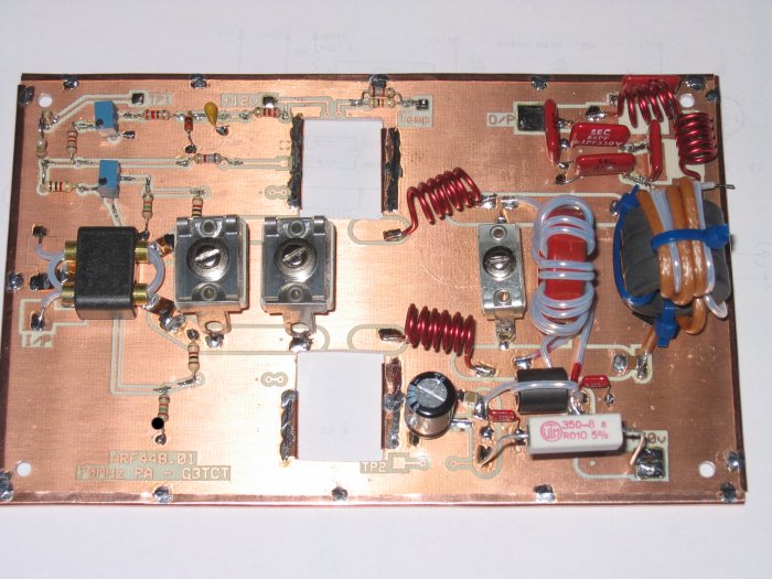
Don't judge this method by the photo above - the D1018 board was produced by a different method. The ARF448 design pictured below was produced by the method above and is much better.